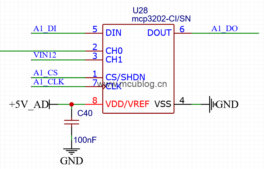
之前介绍过使用STM32的AD采样功能,采集外部电压。这次介绍AD转换芯片MCP3202,是美国MICROCHIP公司推出的一款双通道、12位分辨率的AD采样芯片。外部提供了SPI接口(支持00模式和11模式),可以实现数据的快速读取。芯片原理图如下:
虽然提供了SPI接口,但读取数据时,会发现并不是标准的SPI接口。如果使用的是MCU,参照这个时序图:
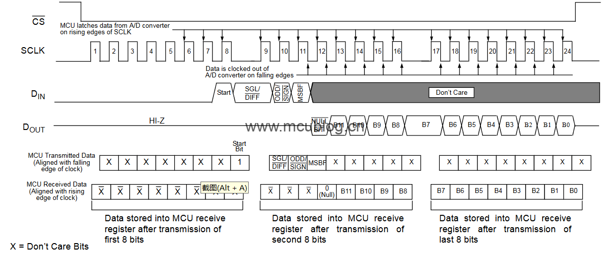
如果使用的是FPGA,参照这个时序图:
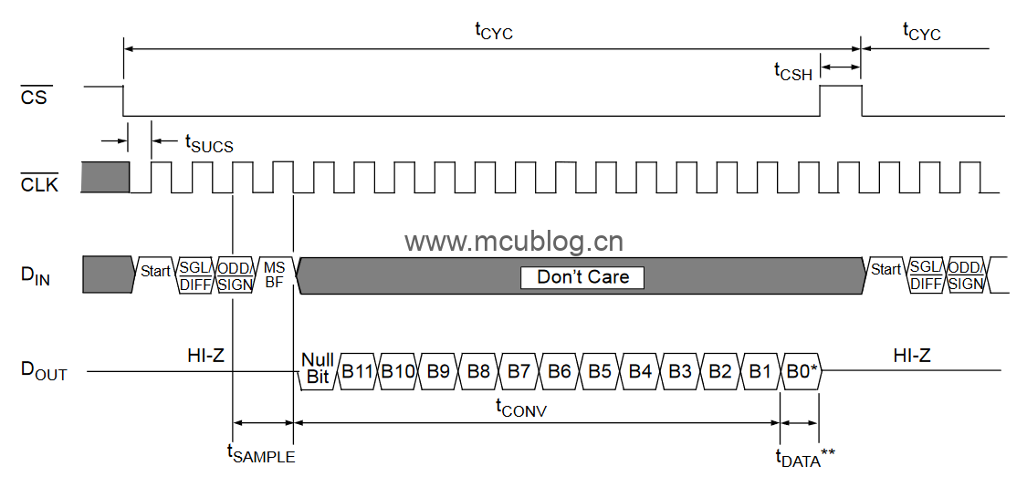
本文只说FPGA方面,所以看第二个图(上图)。从图中可知,当片选(CS)拉低以后,CLK提供了17个时钟,是的,不是8个,不是16个,是17个,这就是为什么说它不是标准的SPI接口。
拉低后,第一个时钟内,DIN提供高电平,告诉芯片开始转换;
第二、第三个时钟,配置高低电平,选择相应的通道(通道0、通道1)、模式(单端、差分)。
第四个时钟,配置数据是高位在前(MSB)还是低位在前(LSB)。
第五个时钟,空的,啥都不用管。
后面12个时钟,DIN上面的电平就无所谓了,只看DOUT上面的电平,它代表AD采样的数据。
搞明白它的工作方式,就可以开始写代码了。
首先写一段代码,提供18个时钟,及相应的CS信号。
为什么是18个?不是17个吗?
因为每次转换完成之后,CS要拉高持续一段时间,这个时间刚好可以用一个CLK来抵消。因此时钟及CS在这里完成。
--串行数据所需时钟的各个状态
type SclkState is (SclkS0 , SclkS1);		--SclkS0:初始化  SclkS1建立17个脉冲
signal SclkSt	:	SclkState := SclkS0;					--设置当前状态为SclkS0

--AD工作状态
type AdState is (AdS0 , AdS1 , AdS2 , AdS3 , AdS4 , AdS5 , AdS6 , AdS7 , AdS8);				--AdS0:启动转换  S1:等待转换  S2:接收数据  S3:锁存数据
signal	AdSt	:	AdState := AdS0;						--设置当前状态为AdS0

signal SclkTmp		:	std_logic := '0';								--串行时钟临时信号
signal CsTmp		:	std_logic := '1';								--片选临时信号
signal	Ad12		:	std_logic_vector (11 downto 0);					--Ad转换值


begin

--SclkTmp 状态机 建立读串行数据时钟18个方波脉冲
	process (Clk)
	variable Cnt		:	std_logic_vector (9 downto 0) := (others => '0');	--读数据时钟半波计数器
	variable SclkCnt	:	std_logic_vector (4 downto 0) := "10010";			--读数据时钟数量计数器
	constant SclkPw		:	std_logic_vector (9 downto 0) := "1111101000"; 			--串行时钟半周期计数值(必须>=2);计1000个Clk时钟、10us,频率50khz

	begin
		if (Clk 'event and Clk = '1') then
			case SclkSt is
				when SclkS0 =>
					Cnt := (others => '0');	--计数器清零
					SclkCnt := "10010";		--数量计数器初始值为18
					SclkTmp <= '0';			--串行时钟变低
					CsTmp <= '0';				--片选拉低
					SclkSt <= SclkS1;
				when SclkS1 =>					--产生18个串行时钟方波
					if (Cnt < SclkPw - 1) then		--小于半波宽度
						Cnt := Cnt + 1;
					else
						Cnt := (others => '0');	--产生前17个串行时钟
						if (Sclkcnt > 2) then	--前16个时钟
							SclkTmp <= not (SclkTmp);
							if (SclkTmp = '1')then
								SclkCnt := SclkCnt - 1;
							end if;
						elsif (Sclkcnt = 2) then	--第17个时钟
							SclkTmp <= not (SclkTmp);
							if (SclkTmp = '1')then
								SclkCnt := SclkCnt - 1;
								CsTmp <= '1';				--片选拉高
							end if;
						else					--第18个串行时钟,维持CS高电平
							if (SclkTmp = '1')then
								SclkSt <= SclkS0;
							end if;
							SclkTmp <= not (SclkTmp);
						end if;
					end if;
			end case;
		end if;
	end process;
	AdSclk <= SclkTmp;							--将串行时钟送到AdSclk引脚
	AdCs <= CsTmp;
接下来写一段程序,按照时钟的上升沿、下降沿,去配置DIN、读取DOUT即可。
	--AD 状态机
	process (Clk)
	variable Sts	:	std_logic_vector (1 downto 0);
	variable Cnt	:	std_logic_vector (4 downto 0);
	variable AdData	:	std_logic_vector (11 downto 0);				--AD串行数据
	constant RcW	:	std_logic_vector (1 downto 0) := "11";		--启动转换Rc低电平宽度。占3个时钟、60ns

	begin
		if (Clk 'event and Clk = '1') then
			case AdSt is
				when AdS0 =>					--开始
					Sts := "00";
					Cnt := (others => '0');
					AdSt <= AdS1;
				when AdS1 =>					--等待CS下降沿
					Sts := Sts (0) & CsTmp;
					if (Sts = "10") then
						--Cnt := (others => '0');
						AdDi <= '1';			--启动转换  START
						AdSt <= AdS2;			--下个CLK
					end if;
				when AdS2 =>
					Sts := Sts (0) & SclkTmp;
					if (Sts = "10") then
						AdDi <= '1';			--选择通道0  SGL
						AdSt <= AdS3;			--下个CLK
					end if;
				when AdS3 =>
					Sts := Sts (0) & SclkTmp;
					if (Sts = "10") then
						AdDi <= '0';			--选择通道0  ODD
						AdSt <= AdS4;			--下个CLK
					end if;
				when AdS4 =>
					Sts := Sts (0) & SclkTmp;
					if (Sts = "10") then
						AdDi <= '1';			--高位在前  MSB
						AdSt <= AdS5;			--下个CLK
					end if;
				when AdS5 =>
					Sts := Sts (0) & SclkTmp;
					if (Sts = "10") then
						AdDi <= '1';			--空位
						AdSt <= AdS6;			--下个CLK
					end if;
				when AdS6 =>
					Sts := Sts (0) & SclkTmp;
					if (Sts = "10") then
						AdSt <= AdS7;			--下个CLK
					end if;
				when AdS7 =>					--接收数据(串行时钟上升沿收取)
					Sts := Sts (0) & SclkTmp;
					if (Sts = "01") then
						AdData := AdData (10 downto 0)& AdDo;
						if (Cnt < "1011") then
							Cnt := Cnt + 1;
						else
							AdSt <= AdS8;
						end if;
					end if;
				when AdS8 =>					--锁存数据
					Ad12 <= AdData;
					AdSt <= AdS0;
			end case;
		end  if;
	end process;
	AdQ <= Ad12;
外部时钟频率100MHZ,内部降频到了50KHZ,代码已验证。可以直接拿去用,也可以在此基础上做一定的修改。
打完收工!